Name: | SW-LAB |
Location: | CEITEC Brno University of Technology |
Instrument description: | LAB enables further miniaturization for proximity, projection, laser and electron beam lithography in one platform for applications such as IC manufacturing, flat panel display, LED, MEMS, 3D packaging, mask manufacturing and nano-fabrication. The fast and accurate calculation of the intensity image enables layout optimization (OPC), mask layout verification, optimization of process conditions (e.g. illumination, stack) and process window (e.g. gap or defocus and exposure dose variation) by varying the layout and/or exposure parameters. Thousands of experiments can be computed "overnight" without producing masks or "burning" wafers. Once a good image contrast has been obtained, 3D resist development modeling allows further optimization of the resist profiles. Complex process effects such as lateral development, density dependent bias in e-beam or in laser lithography can be analyzed and compensated. |
Research group: | CF: CEITEC Nano |
If you would like to use this equipment contact the administrator: |
---|
29. ledna 2018 9:46
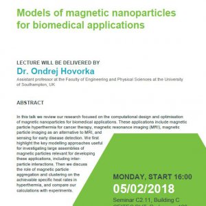
LECTURE: Dr. Ondrej Hovorka: Models of magnetic nanoparticles for biomedical applications
25. ledna 2018 18:21
WHEN: 30. 01. 2018 WHERE: CEITEC BUT, Purkynova 123, large meeting room SPEAKER: Dr Andriy Marko TALK: Advances in PELDOR…