Programme Description
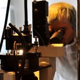
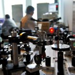
The research is focused on the area of nanotechnologies covering materials and structures to be exploited in nanoelectronic and nanophotonic applications. The research involves the preparation, characterization and analysis of the properties of nanostructures enabling active application of principles, which determine unique and specific properties of nanostructures. Attention will be paid to the research of 2D – OD nanostructures produced by lithographic (top-down) methods and self-organizing (bottom-up) methods. The research will consider semiconductor nanostructures, magnetic and metallic nanostructures, nanotubes and nanofibres, supra-molecules and nano-electronic material on the edge of Moore’s law etc.
Main Goals
The principal goal of this program is to develop methods for the creation of nanostructures, to learn their unique properties and to utilise them in electronics, optoelectronics and photonics. To meet this goal, shared clean-room laboratories equipped with planar technologies and the state-of-the art-diagnostic techniques will be built. Such a facility will be at the disposal not only for research groups from CEITEC but for external groups from academic institutions and industry as well. In this way it will contribute to the widening of cooperation on application subjects within the Czech Republic and Central European region.
Research Groups
- Josef Humlíček Research Group (Functional Properties of Nanostructures)
- Smart Nanodevices
- Experimental Biophotonics
- Fabrication and Characterisation of Nanostructures
- Development of Methods for Analysis and Measuring
- Materials Characterization and Advanced Coatings
- Lenka Zajíčková Research Group (Plasma Technologies)
- Jiří Pinkas Research Group (Synthesis and Analysis of Nanosructures)
- Multiscale Modelling and Measurements of Physical Properties


