Change institution
Advanced Nano and Microtechnologies Advanced Materials Structural Biology Gen. and Prot. of Plant Systems Molecular Medicine Brain and Mind Research Molecular Vet. Medicine

Fabrication and Characterisation of Nanostructures - Tomáš Šikola

Research Group Leader
Researcher ID
Phone: +420 54114 2707
E-mail:
Office:
Deputy Group Leader
Phone: +420 54114 2848
E-mail: ,
Office:

Research areas

  • Fabrication of nanostructures using bottom-up methods
  • Fabrication of nanostructures using top-down methods (nanolithography)
  • Investigation of the functional properties of nanostructures
  • The development of analytical and measurement methods

Main objectives

Fabrication of nanostructures using bottom-up and top-down methods (nanolithography)

Development of methods for the fabrication of nanostructures: planar physical and plasmochemical methods using EBL, UV lithography, FIB, SPM lithography, and imprint technology. MBE, CVD, ALD, PECVD, hybrid methods for selective growths, etc. All the methods developed are utilized directly for fabrication of nanostructures, advanced planar materials and devices.

Investigation of the functional properties of nanostructures

Specification and optimization of the functional properties of nanostructures for nanoelectronics, nanophotonics and (bio)sensing their correlation with geometrical/structural parameters of nanostructures and operational parameters. Novel and unique properties of nanostructures not observable in conventional materials and microstructures open the ways for qualitatively new applications.

Research and development of analytical and measurement methods

Development of techniques and methodologies for microscopy, analysis and metrology of nanomaterials/nanostructures, and for diagnostics of their properties – new techniques of nanometrology by SPM, optical methods, combination of more techniques (SEM, AFM, etc.). This will be used to meet the other objectives of the Advanced Nanotechnologies and Microtechnologies Research Programme and for the characterization of nano- and microstructures generally.

Content of research

Fabrication of nanostructures using bottom-up methods

Fabrication of nanostructures using planar technologies

Research and utilization of phenomena essential for the growth of (ultra)thin films and self-assembling of nanoobjects (nanofibres, nanotubes, nanodots etc.) with specific properties using PVD (MBE, IBAD, magnetron sputtering), CVD, PECVD and (electro)chemical methods. Attention will be paid both to the study of the initial stages of the growth of thin films and nanostructures that are of vital importance for the parameters and properties of the final products (substrate influence, nucleation, diffusion, growth modes, catalytic activity), and to finding relationships between the parameters and the properties of these products. Selective and guided growth of nanostructures on the substrates patterned by lithographic methods.

Research on the fabrication of nanofibres (especially metallic) from electrolytic solutions using e.g. polymeric and alumina matrices and the development of methods of assembling nanofibres using electrophoresis, etc.

Fabrication of nanostructures using top-down methods (nanolithography)

The development of nanolithographic methods by means of electron beam lithography, scanning probe microscopy (e.g. local anodic oxidation), focussed ion beam and their combinations with planar technologies (e.g. selective and guided growth, respectively) for the fabrication of nanostructures with minimum dimensions as close to 10 nm as possible.

  • Fabrication of nanoelements and nanodevices (quantum point contacts, rings and dots, SETs, spintronics systems, etc.)
  • Fabrication of ordered metallic nanoparticles, elements and systems (plasmonics, resonance plasmonic antennas, etc.)
  • Fabrication of ordered dielectric and semiconductor nanodots and nanowires (photonics, optoelectronics, bioactive surfaces)
  • Fabrication of metallic nanoelectrodes for making contacts to molecular nanostructures and nanoelements
  • Fabrication of novel masks (e.g. from SAM), the application of self-assembling and electrochemical methods

 sikola 1


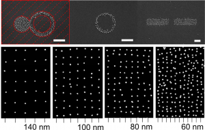
Selective deposition of Au coloids
Negative (top) and positive (bottom) deposition of 20 nm gold nanoparticles after patterning Si substrate with Ga ion beam and immersion in the 3mM HF-modified Au colloidal solution.


Investigation of the functional properties of nanostructures

The main goal is to find correlations between the properties and the geometrical and structural parameters of nanostructures and to use this knowledge for feedback in the technology of their preparation and for various applications.


Magnetic nanostructures

The fabrication of magnetic 2D-0D ordered nanostructures and ultrathin-layered structures utilizing the combination of 3D metals and nonmagnetic materials. An experimental and theoretical study of magnetic anisotropy, transport properties (e.g. GMR, TMR) and the dynamics of domain walls and vortexes for applications in magnetic recording, sensing and spintronics.
 
sikola 2

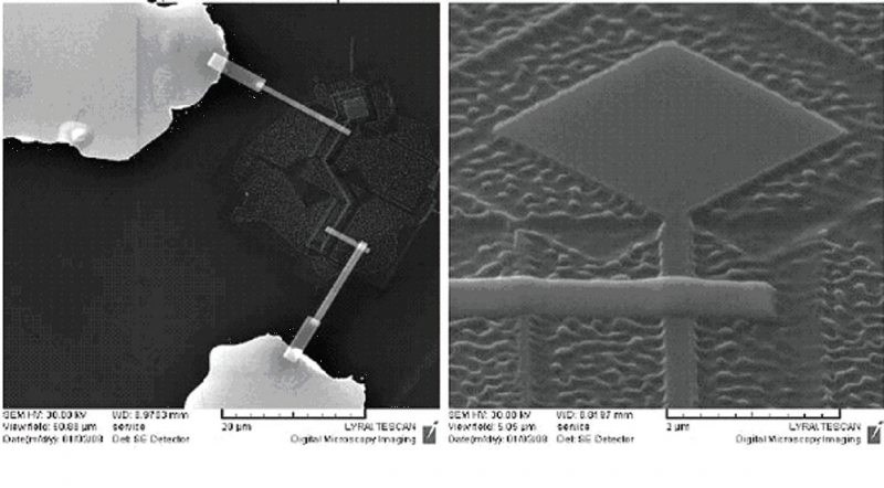
Spin valve nanowires

Nanostructures for plasmonics

The fabrication and study of the properties of metallic nanostructures and microstructures suitable for plasmonics. Research on the generation, detection and application of surface plasmon polaritons. Simulation and experimental verification of localized surface resonances (localized surface plasmons) on metallic nanoparticles, nanowires and nano/micro antennas. The influence of dielectric materials (spacers) between metallic components of plasmonic structures. Applications in micro and nanosensors (including biosensors).

sikola 3
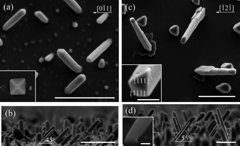
Top and side views of Ge NWs grown on Ge(100) and Ge(111) substrates.
The scale bars represent 1 mm, in insets 200 nm.

Ultrathin films and nanostructures of wide-band gap semiconductors

The fabrication of semiconductor nitride ultrathin films and nanostructures (GaN, AlN) at low and medium temperatures. A study of their electronic structures. The electric transport properties and optoelectronic properties of 0D nanostructures.

Research group SITE

list / cards

Name and position

E-mail

Phone

Filip Ligmajer
Ph.D. student
+420 54114 3349
Pavel Procházka
Ph.D. student
+420 54114 2817
Jakub Sadílek
Ph.D. student
+420 54114 2788, +420 777 176 639
Kirill Andrejevič Ermakov
Ph.D. student
, +420 774 191 329
Martin Hrtoň
Ph.D. student
, +420 739 159 589
Martin Konečný
Ph.D. student
Prof. Tomáš Šikola
Research Program Coordinator
+420 54114 2707
Prof. Jiří Spousta, Ph.D.
Senior Researcher
+420 54114 2848
Michal Kvapil, Ph.D.
Junior researcher
+420 54114 3349
Miroslav Kolíbal, Ph.D.
Junior Researcher
+420 54114 9243
Vlastimil Křápek, Ph.D.
Junior Researcher
+420 54114 2810
Zuzana Lišková, Ph.D.
Core Facility Operator
+420 54114 9217
Jindřich Mach, Ph.D.
Junior Researcher
+420 54114 2813
Věra Melkesová
Administrative Support
+420 54114 2823
Michal Potoček, Ph.D.
Junior Researcher
+420 54114 2814, +420 726 812 814
Josef Polčák, Ph.D.
Core facility operator
+420 54114 9213
Stanislav Průša, Ph.D.
Senior Researcher
+420 54114 2832, +420 732 113 816
Tomáš Šamořil
Core facility operator
+420 54114 9214, +420 724 228 591
Dalibor Šulc, Ph.D.
Core facility operator
+420 54114 9257
Michal Urbánek, Ph.D.
CEITEC Nano Group leader
+420 54114 9200
Vojtěch Uhlíř, Ph.D.
Junior Researcher
+420 54114 9220
Stanislav Voborný, Ph.D.
Junior Researcher
+420 54114 2783
Prof. Peter Varga
Senior Researcher
Jakub Zlámal, Ph.D.
Junior Researcher
+420 54114 2788
Oto Lipovský
Support Staff
+420 54114 2834
Tomáš Pejchal
Ph.D. student
Bruno Sedláček
Support Staff
+420 54114 2784
Jitka Strouhalová
Technician
Petr Bábor, Ph.D.
Junior Researcher
+420 54114 2783
Miroslav Bartošík, Ph.D.
Junior Researcher
+420 54114 2814
Eva Kolíbalová, Ph.D.
Core facility operator
+420 54114 9215
Lukáš Flajšman
Ph.D. student
Jan Čechal, Ph.D.
Junior researcher group leader
+420 54114 2810
Michal Horák
Ph.D. student
Michal Horký
Ph.D. student
Meena Dhankhar
Ph.D. student
+420 51414 2849
Libuše Dittrichová
Junior Researcher
+420 54114 2829
Prof. Petr Dub
Senior Researcher
+420 54114 2708
Vítězslav Duma
Support Staff
+420 54114 2784
Marek Vaňatka
Ph.D. student
Radek Kalousek, Ph.D.
Senior Researcher
+420 54114 2783
Jan Neuman, Ph.D.
Junior researcher
+420 54114 2779, +420 54114 2779
Dana Chatrná
Administrative Support
+420 54114 2821
Michal Pavera, Ph.D.
Junior researcher
+420 54114 2811
Petr Skalka, Ph.D.
Junior Researcher
+420 54114 2869
Jiří Babocký
Ph.D. student
Jon Ander Arregi Uribeetxebarria
Junior researcher
Zoltán Édes
Ph.D. student
Jiří Liška
Junior researcher
Lukáš Kormoš
Ph.D. student
Jakub Piastek
Ph.D. student
Vojtěch Švarc
Core Facility operator
+420 54114 9257
Michal Kotoul
Senior Researcher
+420 54114 2889, +420 54114 5206
Jaroslav Maniš
Ph.D. student
Lukáš Kejík
Ph.D. student
Lukáš Kachtík
Ph.D. student
Anton Olegovich Makoveev
laboratory technician
Ondřej Metelka
Miloš Hrabovský
Božena Čechalová
project manager
+420 54114 9261
Jakub Hrubý
Ph.D. student
Antonín Sojka
Ph.D. student
Artur Solodovnyk
Ph.D. student
Michal Staňo
junior researcher
Viktor Badin
Laboratory technician
Zdeněk Nováček
Junior researcher
+420 54114 2811, +420 54114 2782
Jakub Piastek
Artur Solodovnyk
Ph.D. student

SELECTED PUBLICATIONS

2017

  • BABOCKY, J; KRIZOVA, A; STRBKOVA, L; KEJIK, L; LIGMAJER, F; HRTON, M; DVORAK, P; TYC, M; COLLAKOVA, J; KRAPEK, V; KALOUSEK, R; CHMELIK, R; SIKOLA, T, 2017:Quantitative 3D Phase Imaging of Plasmonic Metasurfaces. ACS PHOTONICS 4 (6), p. 1389 - 1397.
  • CECHAL, J; SIKOLA, T, 2017:Flexible foils formed by a prolonged electron beam irradiation in scanning electron microscope. APPLIED SURFACE SCIENCE 423 , p. 538 - 541.
  • DVORAK, P; EDES, Z; KVAPIL, M; SAMORIL, T; LIGMAJER, F; HRTON, M; KALOUSEK, R; KRAPEK, V; DUB, P; SPOUSTA, J; VARGA, P; SIKOLA, T, 2017:Imaging of near-field interference patterns by aperture-type SNOM - influence of illumination wavelength and polarization state. OPTICS EXPRESS 25 (14), p. 16560 - 16573.
  • HE, JJ; ZHENG, W; LIGMAJER, FL; CHAN, CF; BAO, ZY; WONG, KL; CHEN, XY; HAO, JH; DAI, JY; YU, SF; LEI, DY, 2017:Plasmonic enhancement and polarization dependence of nonlinear upconversion emissions from single gold nanorod@SiO2@CaF2:Yb3+,Er3+ hybrid core-shell-satellite nanostructures. LIGHT-SCIENCE & APPLICATIONS 6
  • HRDY, R; KYNCLOVA, H; KLEPACOVA, I; BARTOSIK, M; NEUZIL, P, 2017:Portable Lock-in Amplifier-Based Electrochemical Method to Measure an Array of 64 Sensors for Point-of-Care Applications. ANALYTICAL CHEMISTRY 89 (17), p. 8731 - 8737.
  • HRTON, M; KRAPEK, V; SIKOLA, T, 2017:Boundary element method for 2D materials and thin films. OPTICS EXPRESS 25 (20), p. 23709 - 23724.
  • KALOUSEK, R; SPOUSTA, J; ZLAMAL, J; DUB, P; SIKOLA, T; SHEN, ZJ; SALAMON, D; MACA, K, 2017:Rapid heating of zirconia nanoparticle-powder compacts by infrared radiation heat transfer. JOURNAL OF THE EUROPEAN CERAMIC SOCIETY 37 (3), p. 1067 - 1072.
  • MANAKHOV, A; CECHAL, J; MICHLICEK, M; SHTANSKY, DV, 2017:Determination of NH2 concentration on 3-aminopropyl tri-ethoxy silane layers and cyclopropylamine plasma polymers by liquid-phase derivatization with 5-iodo 2-furaldehyde. APPLIED SURFACE SCIENCE 414 , p. 390 - 397.
  • MANAKHOV, A; LANDOVA, M; MEDALOVA, J; MICHLICEK, M; POLCAK, J; NECAS, D; ZAJICKOVA, L, 2017:Cyclopropylamine plasma polymers for increased cell adhesion and growth. PLASMA PROCESSES AND POLYMERS 14 (7)
  • PROCHAZKA, P; MARECEK, D; LISKOVA, Z; CECHAL, J; SIKOLA, T, 2017:X-ray induced electrostatic graphene doping via defect charging in gate dielectric. SCIENTIFIC REPORTS 7

2016

  • CECHAL, J; KLEY, CS; PETUYA, R; SCHRAMM, F; RUBEN, M; STEPANOW, S; ARNAU, A; KERN, K, 2016:CO2 Binding and Induced Structural Collapse of a Surface-Supported Metal-Organic Network. JOURNAL OF PHYSICAL CHEMISTRY C 120 (33), p. 18622 - 18630.
  • ELBADAWI, C; TRAN, TT; KOLIBAL, M; SIKOLA, T; SCOTT, J; CAI, QR; LI, LH; TANIGUCHI, T; WATANABE, K; TOTH, M; AHARONOVICH, I; LOBO, C, 2016:Electron beam directed etching of hexagonal boron nitride. NANOSCALE 8 (36), p. 16182 - 16186.
  • GABLECH, I; SVATOS, V; CAHA, O; HRABOVSKY, M; PRASEK, J; HUBALEK, J; SIKOLA, T, 2016:Preparation of (001) preferentially oriented titanium thin films by ion-beam sputtering deposition on thermal silicon dioxide. JOURNAL OF MATERIALS SCIENCE 51 (7), p. 3329 - 3336.
  • KOLIBAL, M; NOVAK, L; SHANLEY, T; TOTH, M; SIKOLA, T, 2016:Silicon oxide nanowire growth mechanisms revealed by real-time electron microscopy. NANOSCALE 8 (1), p. 266 - 275.
  • KOLIBAL, M; PEJCHAL, T; VYSTAVEL, T; SIKOLA, T, 2016:The Synergic Effect of Atomic Hydrogen Adsorption and Catalyst Spreading on Ge Nanowire Growth Orientation and Kinking. NANO LETTERS 16 (8), p. 4880 - 4886.
  • MANAKHOV, A; MAKHNEVA, E; SKLADAL, P; NECAS, D; CECHAL, J; KALINA, L; ELIAS, M; ZAJICKOVA, L, 2016:The robust bio-immobilization based on pulsed plasma polymerization of cyclopropylamine and glutaraldehyde coupling chemistry. APPLIED SURFACE SCIENCE 360 , p. 28 - 36.
  • MANAKHOV, A; MICHLICEK, M; NECAS, D; POLCAK, J; MAKHNEVA, E; ELIAS, M; ZAJICKOVA, L, 2016:Carboxyl-rich coatings deposited by atmospheric plasma co-polymerization of maleic anhydride and acetylene. SURFACE & COATINGS TECHNOLOGY 295 , p. 37 - 45.
  • PESL, M; PRIBYL, J; ACIMOVIC, I; VILOTIC, A; JELINKOVA, S; SALYKIN, A; LACAMPAGNE, A; DVORAK, P; MELI, AC; SKLADAL, P; ROTREKL, V, 2016:Atomic force microscopy combined with human pluripotent stem cell derived cardiomyocytes for biomechanical sensing. BIOSENSORS & BIOELECTRONICS 85 , p. 751 - 757.
  • PODUSKA, J; HUTAR, P; KUCERA, J; FRANK, A; SADILEK, J; PINTER, G; NAHLIK, L, 2016:Residual stress in polyethylene pipes. POLYMER TESTING 54 , p. 288 - 295.
  • ROZBORIL, J; RECHKEMMER, Y; BLOOS, D; MUNZ, F; WANG, CN; NEUGEBAUER, P; CECHAL, J; NOVAK, J; VAN SLAGEREN, J, 2016:Magneto-optical investigations of molecular nanomagnet monolayers. DALTON TRANSACTIONS 45 (18), p. 7555 - 7558.
  • SALAMON, D; KALOUSEK, R; ZLAMAL, J; MACA, K, 2016:Role of conduction and convection heat transfer during rapid crack-free sintering of bulk ceramic with low thermal conductivity. JOURNAL OF THE EUROPEAN CERAMIC SOCIETY 36 (12), p. 2955 - 2959.
  • SIK, O; BABOR, P; SKARVADA, P; POTOCEK, M; TRCKA, T; GRMELA, L; BELAS, E, 2016:Investigation of the effect of argon ion beam on CdZnTe single crystals surface structural properties. SURFACE & COATINGS TECHNOLOGY 306 , p. 75 - 81.
  • SIMSIKOVA, M; BARTOS, M; CECHAL, J; SIKOLA, T, 2016:Decolorization of organic dyes by gold nanoflowers prepared on reduced graphene oxide by tea polyphenols. CATALYSIS SCIENCE & TECHNOLOGY 6 (9), p. 3008 - 3017.
  • SLAMECKA, K; SKALKA, P; POKLUDA, J; CELKO, L, 2016:Finite element simulation of stresses in a plasma-sprayed thermal barrier coating with an irregular top-coat/bond-coat interface. SURFACE & COATINGS TECHNOLOGY 304 , p. 574 - 583.
  • UHLIR, V; ARREGI, JA; FULLERTON, EE, 2016:Colossal magnetic phase transition asymmetry in mesoscale FeRh stripes. NATURE COMMUNICATIONS 7
  • VALLEJOS, S; PIZUROVA, N; GRACIA, I; SOTELO-VAZQUEZ, C; CECHAL, J; BLACKMAN, C; PARKIN, I; CANE, C, 2016:ZnO Rods with Exposed {100} Facets Grown via a Self-Catalyzed Vapor-Solid Mechanism and Their Photocatalytic and Gas Sensing Properties. ACS APPLIED MATERIALS & INTERFACES 8 (48), p. 33335 - 33342.

2015

  • KRAPEK, V; KOH, AL; BRINEK, L; HRTON, M; TOMANEC, O; KALOUSEK, R; MAIER, SA; SIKOLA, T, 2015:Spatially resolved electron energy loss spectroscopy of crescent-shaped plasmonic antennas. OPTICS EXPRESS 23 (9), p. 11855 - 11867.
  • MANAKHOV, A; NECAS, D; CECHAL, J; PAVLINAK, D; ELIAS, M; ZAJICKOVA, L, 2015:Deposition of stable amine coating onto polycaprolactone nanofibers by low pressure cyclopropylamine plasma polymerization. THIN SOLID FILMS 581 , p. 7 - 13.
  • NEUMAN, T; ALONSO-GONZALEZ, P; GARCIA-ETXARRI, A; SCHNELL, M; HILLENBRAND, R; AIZPURUA, J, 2015:Mapping the near fields of plasmonic nanoantennas by scattering-type scanning near-field optical microscopy. LASER & PHOTONICS REVIEWS 9 (6), p. 637 - 649.
  • SALAMON, D; KALOUSEK, R; MACA, K; SHEN, ZJ, 2015:Rapid Grain Growth in 3Y-TZP Nanoceramics by Pressure-Assisted and Pressure-Less SPS. JOURNAL OF THE AMERICAN CERAMIC SOCIETY 98 (12), p. 3706 - 3712.
  • SLAMECLA, K; CELKO, L; SKALKA, P; POKLUDA, J; NEMEC, K; JULIS, M; KLAKURKOVA, L; SVEJCAR, J, 2015:Bending fatigue failure of atmospheric-plasma-sprayed CoNiCrAlY plus YSZ CrossMark thermal barrier coatings. INTERNATIONAL JOURNAL OF FATIGUE 70 , p. 186 - 195.
  • URBANEK, M; UHLIR, V; LAMBERT, CH; KAN, JJ; EIBAGI, N; VANATKA, M; FLAJSMAN, L; KALOUSEK, R; IM, MY; FISCHER, P; SIKOLA, T; FULLERTON, EE, 2015:Dynamics and efficiency of magnetic vortex circulation reversal. PHYSICAL REVIEW B 91 (9)

2014

  • CECHAL, J; KLEY, CS; KUMAGAI, T; SCHRAMM, F; RUBEN, M; STEPANOW, S; KERN, K, 2014:Convergent and divergent two-dimensional coordination networks formed through substrate-activated or quenched alkynyl ligation. CHEMICAL COMMUNICATIONS 50 (69), p. 9973 - 9976.
  • CECHAL, J; POLCAK, J; SIKOLA, T, 2014:Detachment Limited Kinetics of Gold Diffusion through Ultrathin Oxide Layers. JOURNAL OF PHYSICAL CHEMISTRY C 118 (31), p. 17549 - 17555.
  • KOLIBAL, M; VYSTAVEL, T; VARGA, P; SIKOLA, T, 2014:Real-Time Observation of Collector Droplet Oscillations during Growth of Straight Nanowires. NANO LETTERS 14 (4), p. 1756 - 1761.
  • MANAKHOV, A; SKLADAL, P; NECAS, D; CECHAL, J; POLCAK, J; ELIAS, M; ZAJICKOVA, L, 2014:Cyclopropylamine plasma polymers deposited onto quartz crystal microbalance for biosensing application. PHYSICA STATUS SOLIDI A-APPLICATIONS AND MATERIALS SCIENCE 211 (12), p. 2801 - 2808.
  • MANAKHOV, A; ZAJICKOVA, L; ELIAS, M; CECHAL, J; POLCAK, J; HNILICA, J; BITTNEROVA, S; NECAS, D, 2014:Optimization of Cyclopropylamine Plasma Polymerization toward Enhanced Layer Stability in Contact with Water. PLASMA PROCESSES AND POLYMERS 11 (6), p. 532 - 544.
  • PROCHAZKA, P; MACH, J; BISCHOFF, D; LISKOVA, Z; DVORAK, P; VANATKA, M; SIMONET, P; VARLET, A; HEMZAL, D; PETRENEC, M; KALINA, L; BARTOSIK, M; ENSSLIN, K; VARGA, P; CECHAL, J; SIKOLA, T, 2014:Ultrasmooth metallic foils for growth of high quality graphene by chemical vapor deposition. NANOTECHNOLOGY 25 (18)
  • SHANEL, O; ZLAMAL, J; ORAL, M, 2014:Calculation of the performance of magnetic lenses with limited machining precision. ULTRAMICROSCOPY 137 , p. 1 - 6.
  • SIMSIKOVA, M; CECHAL, J; ZORKOVSKA, A; ANTALIK, M; SIKOLA, T, 2014:CuO/ZnO nanocomposite for colorimetric detection of cysteine. JOURNAL OF BIOLOGICAL INORGANIC CHEMISTRY 19 , p. S877 - S878.

2013

  • ALLSOP, T; NEAL, R; DVORAK, M; KALLI, K; ROZHIN, A; WEBB, DJ, 2013:Physical characteristics of localized surface plasmons resulting from nano-scale structured multi-layer thin films deposited on D-shaped optical fiber. OPTICS EXPRESS 21 (16), p. 18765 - 18776.
  • CECHAL, J; KLEY, CS; KUMAGAI, T; SCHRAMM, F; RUBEN, M; STEPANOW, S; KERN, K, 2013:Functionalization of Open Two-Dimensional Metal-Organic Templates through the Selective Incorporation of Metal Atoms. JOURNAL OF PHYSICAL CHEMISTRY C 117 (17), p. 8871 - 8877.
  • DVORAK, P; NEUMAN, T; BRINEK, L; SAMORIL, T; KALOUSEK, R; DUB, P; VARGA, P; SIKOLA, T, 2013:Control and Near-Field Detection of Surface Plasmon Interference Patterns. NANO LETTERS 13 (6), p. 2558 - 2563.
  • GIESBERS, AJM; PROCHAZKA, P; FLIPSE, CFJ, 2013:Surface phonon scattering in epitaxial graphene on 6H-SiC. PHYSICAL REVIEW B 87 (19), p. 19540 - 1 (5 p.
  • GIESBERS, AJM; UHLIROVA, K; KONECNY, M; PETERS, EC; BURGHARD, M; AARTS, J; FLIPSE, CFJ, 2013:Interface-Induced Room-Temperature Ferromagnetism in Hydrogenated Epitaxial Graphene. PHYSICAL REVIEW LETTERS 111 (16)
  • GLOSS, J; ZAMAN, SS; JONNER, J; NOVOTNY, Z; SCHMID, M; VARGA, P; URBANEK, M, 2013:Ion-beam-induced magnetic and structural phase transformation of Ni-stabilized face-centered-cubic Fe films on Cu(100). APPLIED PHYSICS LETTERS 103 (26)
  • KUNES, J; KRAPEK, V, 2013:Disproportionation and Metallization at Low-Spin to High-Spin Transition in Multiorbital Mott Systems (vol 106, 256401, 2011). PHYSICAL REVIEW LETTERS 110 (1)
  • MIKMEKOVA, E; POLCAK, J; SOBOTA, J; MULLEROVA, I; PERINA, V; CAHA, O, 2013:Humidity resistant hydrogenated carbon nitride films. APPLIED SURFACE SCIENCE 275 (1), p. 7 - 13.
  • NOVOTNY, Z; MULAKALURI, N; EDES, Z; SCHMID, M; PENTCHEVA, R; DIEBOLD, U; PARKINSON, GS, 2013:Probing the surface phase diagram of Fe3O4(001) towards the Fe-rich limit: Evidence for progressive reduction of the surface. PHYSICAL REVIEW B 87 (19), p. 19541 - 1 (8 p.
  • PLUMHOF, JD; TROTTA, R; KRAPEK, V; ZALLO, E; ATKINSON, P; KUMAR, S; RASTELLI, A; SCHMIDT, OG, 2013:Tuning of the valence band mixing of excitons confined in GaAs/AlGaAs quantum dots via piezoelectric-induced anisotropic strain. PHYSICAL REVIEW B 87 (7)
  • SIMSIKOVA, M; ANTALIK, M; KANUCHOVA, M; SKVARLA, J, 2013:Anionic 11-mercaptoundecanoic acid capped ZnO nanoparticles. APPLIED SURFACE SCIENCE 282 , p. 342 - 347.
  • UHLIR, V; URBANEK, M; HLADIK, L; SPOUSTA, J; IM, MY; FISCHER, P; EIBAGI, N; KAN, JJ; FULLERTON, EE; SIKOLA, T, 2013:Dynamic switching of the spin circulation in tapered magnetic nanodisks. NATURE NANOTECHNOLOGY 8 (5), p. 341 - 346.

2012

  • AIT-MANSOUR, K; BRUNE, H; PASSERONE, D; SCHMID, M; XIAO, WD; RUFFIEUX, P; BUCHSBAUM, A; VARGA, P; FASEL, R; GRONING, O, 2012:Interface-confined mixing and buried partial dislocations for Ag bilayer on Pt(111). PHYSICAL REVIEW B 86 (8)
  • ANTLANGER, M; MAYR-SCHMOLZER, W; PAVELEC, J; MITTENDORFER, F; REDINGER, J; VARGA, P; DIEBOLD, U; SCHMID, M, 2012:Pt3Zr(0001): A substrate for growing well-ordered ultrathin zirconia films by oxidation. PHYSICAL REVIEW B 86 (3)
  • GUSTAFSON, J; LUNDGREN, E; MIKKELSEN, A; BORG, M; KLIKOVITS, J; SCHMID, M; VARGA, P; ANDERSEN, JN, 2012:The Rh(100)-(3 x 1)-2O structure. JOURNAL OF PHYSICS-CONDENSED MATTER 24 (22)
  • HRTON, M; POYLI, MA; SILKIN, VM; AIZPURUA, J, 2012:Optical excitation of acoustic surface plasmons in metallic nanoparticles. ANNALEN DER PHYSIK 524 (11), p. 751 - 756.
  • KALOUSEK, R; DUB, P; BRINEK, L; SIKOLA, T, 2012:Response of plasmonic resonant nanorods: an analytical approach to optical antennas. OPTICS EXPRESS 20 (16), p. 17916 - 17927.
  • KLEY, CS; CECHAL, J; KUMAGAI, T; SCHRAMM, F; RUBEN, M; STEPANOW, S; KERN, K, 2012:Highly Adaptable Two-Dimensional Metal-Organic Coordination Networks on Metal Surfaces. JOURNAL OF THE AMERICAN CHEMICAL SOCIETY 134 (14), p. 6072 - 6075.
  • KOLIBAL, M; KALOUSEK, R; VYSTAVEL, T; NOVAK, L; SIKOLA, T, 2012:Controlled faceting in < 110 > germanium nanowire growth by switching between vapor-liquid-solid and vapor-solid-solid growth. APPLIED PHYSICS LETTERS 100 (20)
  • KOLIBAL, M; KONECNY, M; LIGMAJER, F; SKODA, D; VYSTAVEL, T; ZLAMAL, J; VARGA, P; SIKOLA, T, 2012:Guided Assembly of Gold Colloidal Nanoparticles on Silicon Substrates Prepatterned by Charged Particle Beams. ACS NANO 6 (11), p. 10098 - 10106.
  • KRAPEK, V; NOVAK, P; KUNES, J; NOVOSELOV, D; KOROTIN, DM; ANISIMOV, VI, 2012:Spin state transition and covalent bonding in LaCoO3. PHYSICAL REVIEW B 86 (19)
  • KUNES, J; KRAPEK, V; PARRAGH, N; SANGIOVANNI, G; TOSCHI, A; KOZHEVNIKOV, AV, 2012:Spin State of Negative Charge-Transfer Material SrCoO3. PHYSICAL REVIEW LETTERS 109 (11)
  • ROUGEMAILLE, N; UHLIR, V; FRUCHART, O; PIZZINI, S; VOGEL, J; TOUSSAINT, JC, 2012:Phase diagram of magnetic domain walls in spin valve nano-stripes. APPLIED PHYSICS LETTERS 100 (17), p. 17240 - .
  • UHLIR, V; VOGEL, J; ROUGEMAILLE, N; FRUCHART, O; ISHAQUE, Z; CROS, V; CAMARERO, J; CEZAR, JC; SIROTTI, F; PIZZINI, S, 2012:Current-induced domain wall motion and magnetization dynamics in CoFeB/Cu/Co nanostripes. JOURNAL OF PHYSICS-CONDENSED MATTER 24 (2)
  • ZENKYU, R; YUHARA, J; MATSUI, T; ZAMAN, SS; SCHMID, M; VARGA, P, 2012:Composition and local atomic arrangement of decagonal Al-Co-Cu quasicrystal surfaces. PHYSICAL REVIEW B 86 (11)

2011

  • KOLIBAL, M; VYSTAVEL, T; NOVAK, L; MACH, J; SIKOLA, T, 2011:In-situ observation of < 110 > oriented Ge nanowire growth and associated collector droplet behavior. APPLIED PHYSICS LETTERS 99 (14)
  • KUNES, J; KRAPEK, V, 2011:Disproportionation and Metallization at Low-Spin to High-Spin Transition in Multiorbital Mott Systems. PHYSICAL REVIEW LETTERS 106 (25)
  • UHLIR, V; PIZZINI, S; ROUGEMAILLE, N; CROS, V; JIMENEZ, E; RANNO, L; FRUCHART, O; URBANEK, M; GAUDIN, G; CAMARERO, J; TIEG, C; SIROTTI, F; WAGNER, E; VOGEL, J, 2011:Direct observation of Oersted-field-induced magnetization dynamics in magnetic nanostripes. PHYSICAL REVIEW B 83 (2)

2010

  • KLENOVSKY, P; KRAPEK, V; MUNZAR, D; HUMLICEK, J, 2010:Electronic structure of InAs quantum dots with GaAsSb strain reducing layer: Localization of holes and its effect on the optical properties. APPLIED PHYSICS LETTERS 97 (20)
  • KOH, AL; TOMANEC, O; URBANEK, M; SIKOLA, T; MAIER, SA; MCCOMB, DW, 2010:HRTEM and EELS of nanoantenna structures fabricated using focused ion beam techniques. ELECTRON MICROSCOPY AND ANALYSIS GROUP CONFERENCE 2009 (EMAG 2009) 241
  • URBANEK, M; UHLIR, V; BABOR, P; KOLIBALOVA, E; HRNCIR, T; SPOUSTA, J; SIKOLA, T, 2010:Focused ion beam fabrication of spintronic nanostructures: an optimization of the milling process. NANOTECHNOLOGY 21 (14)

GRANTY

  • Self-organized functional layers of molecular quantum bits (7AMDE005), DAAD, 2015 - 2016
  • Manufacture of magnetic metamaterials using a direct entry focused ion beam (GA15-62503S), Czech Science Foundation - International Projects, 2015 - 2017
  • Mapping of localized plasmon resonances at nanoantennas (GAP102/12/1881), Czech Science Foundation - Standard Grants, 2012 - 2014
  • Fabrication of metallic nanostructures for spintronic applications (GPP102/12/P443), Czech Science Foundation - Postdoc Grants, 2012 - 2014
  • Fabrication of semiconductor nanowires with optimized functional properties (GPP108/12/P699), Czech Science Foundation - Postdoc Grants, 2012 - 2014
  • Advanced microscopy and spectroscopy platform for research and development in nano and microtechnologies – AMISPEC (TE01020233), Technology Agency of the Czech Rep. - Centres of Competence, 2012 - 2019

CURRENT RESEARCH INFRASTRUCTURE

The experimental facilities of the group are mainly located in clean rooms (class < 100 000). They include the following equipment:

Dual ion beam HV apparatus for ion-beam assisted deposition and ion-beam etching; complex UHV apparatus for deposition and in situ analysis of ultrathin films with four effusion cells for molecular beam deposition, a hyperthermal ion-beam source for direct ion beam deposition, and surface analytical techniques (SIMS, TOF-LEIS, XPS, TDS, LEED, RHEED, spectroscopic ellipsometry); two commercial scanning probe microscopes (AutoProbe Veeco, NT-MDT Ntegra) providing various modes such as AFM, LFM, conductive AFM, EFM, Kelvin probe, nanolithography mode and in case of NT-MDT microscope also a near field mode (SNOM) providing illumination and collection operational regimes both in reflection or transmission (inverted microscope) measuring schemes; FIB system (Tescan Mira), microreflection spectrometer; a setup for magnetooptical Kerr effect, etc. Other instruments such as standard and confocal optical microscopes and a scanning electron microscope with a lithographic option (Tescan – Vega) are available in the labs outside of the clean rooms.

More CEITEC News ...
Dr. Ondrej Hovorka: Models of magnetic nanoparticles for biomedical applications

29. ledna 2018 9:46

Dr. Ondrej Hovorka: Models of magnetic nanoparticles for biomedical…

LECTURE: Dr. Ondrej Hovorka: Models of magnetic nanoparticles for biomedical applications

Advanced Materials and Nanotechnology Seminar Series 2018: Dr Andriy Marko

25. ledna 2018 18:21

Advanced Materials and Nanotechnology Seminar Series 2018: Dr Andriy…

WHEN: 30. 01. 2018 WHERE: CEITEC BUT, Purkynova 123, large meeting room SPEAKER: Dr Andriy Marko TALK: Advances in PELDOR…